Semiconductor Wafer: Key Points
- Wafer thickness affects thermal management, yield, and how the wafer behaves during fabrication
- While silicon remains the industry standard, advanced applications are turning to SOI, GaAs, SiC, and GaN wafers for greater speed, efficiency, and heat resistance
- Factors like flatness, resistivity, crystal orientation, and surface defects all influence the final device performance
- From EVs and 5G to solar cells and aerospace electronics, wafer selection is tightly aligned with industry-specific demands
The thickness, type, and material quality of semiconductor wafers directly impact how fast a chip runs, how much power it uses, and how reliable it is over time.
With global demand for advanced semiconductors continuing to rise, understanding these properties is more essential than ever for design engineers, manufacturers, and sourcing teams.
In this guide, we’ll break down:
- How wafer thickness is measured and why it matters
- The difference between silicon, SOI, and compound wafers
- What makes a wafer high-quality from a fabrication perspective
- Industry use cases for thin, thick, and specialty wafers
Semiconductor Wafer Thickness Explained
While semiconductor wafer thickness might seem like a minor detail, it plays a major role in high-precision electronics, manufacturing and packaging, and their performance in real-world conditions.
From mechanical strength to heat dissipation, the thickness of a wafer directly affects the yield, reliability, and end-use of a semiconductor device.
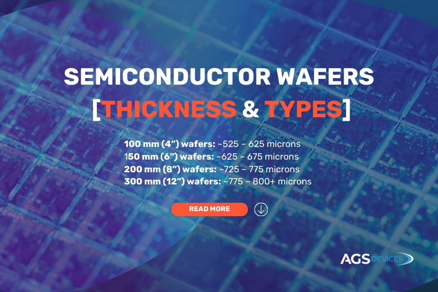
Standard Wafer Thicknesses by Diameter
Wafers come in standard diameters — commonly 100 mm (4″), 150 mm (6″), 200 mm (8″), and 300 mm (12″).
Each diameter has a general thickness range:
- 100 mm (4”) wafers: ~525–625 microns
- 150 mm (6”) wafers: ~625–675 microns
- 200 mm (8”) wafers: ~725–775 microns
- 300 mm (12”) wafers: ~775–800+ microns
How Thickness Impacts Manufacturing and Performance
Wafer thickness is closely tied to fabrication efficiency and mechanical handling due to:
- Mechanical stability: Thicker wafers are less likely to crack during photolithography and etching, especially in older fabs using manual handling or older tooling.
- Thermal management: Thicker substrates help dissipate heat more effectively, critical in high-power or high-frequency applications.
- Back-end processing: During back grinding (the thinning of wafers before packaging), maintaining precise thickness is key to preventing wafer warping or delamination.
- Packaging compatibility: Thinner wafers are easier to integrate into compact or stacked packaging solutions, like 3D ICs or high-density memory modules.
Applications Requiring Ultra-Thin vs. Thick Wafers
Ultra-thin wafers that are less than 200 microns are often used in:
- Smartphones and wearables: Where space is limited and weight is critical.
- 3D ICs and TSVs (Through-Silicon Vias): Where they’re mostly used for vertical chip stacking.
- MEMS devices and sensors: Since they require flexibility or close integration.
Thicker wafers, on the other hand, are preferred for:
- Power electronics: Such as those used in electric vehicles or industrial motor control.
- RF and microwave devices: Where thermal performance and strength are essential.
- Legacy systems: That require rigid substrates for robustness and mechanical alignment.

Types of Semiconductor Wafers and Their Properties
Semiconductor wafers aren’t one-size-fits-all. The type of wafer used directly impacts the electrical, thermal, and structural characteristics of the final device.
From standard silicon to high-performance compound materials, selecting the right wafer type is foundational to system efficiency and reliability.
Silicon Wafers: Float-Zone vs. Czochralski
Silicon remains the most widely used material in semiconductor electronics manufacturing due to its abundance, cost-effectiveness, and well-established processing ecosystem.
But not all silicon wafers are created the same — two primary production methods create distinct material characteristics.
Float-Zone (FZ) Silicon:
Created by melting a narrow region of a silicon rod and moving it along the ingot to purify the crystal.
FZ wafers offer extremely low impurity levels and high resistivity, making them ideal for:
- Power semiconductors
- High-voltage diodes
- RF devices where purity impacts signal integrity
Use case: Float-Zone (FZ) silicon is commonly used in high-voltage power modules found in electric trains and industrial motor drives.
Czochralski (CZ) Silicon:
More commonly used in commercial chip production, CZ wafers are pulled from molten silicon in a crucible.
While they contain more oxygen and impurities than FZ wafers, they are:
- Cost-efficient
- Scalable for large-diameter wafers
- Suitable for logic ICs, memory chips, and general-purpose electronics
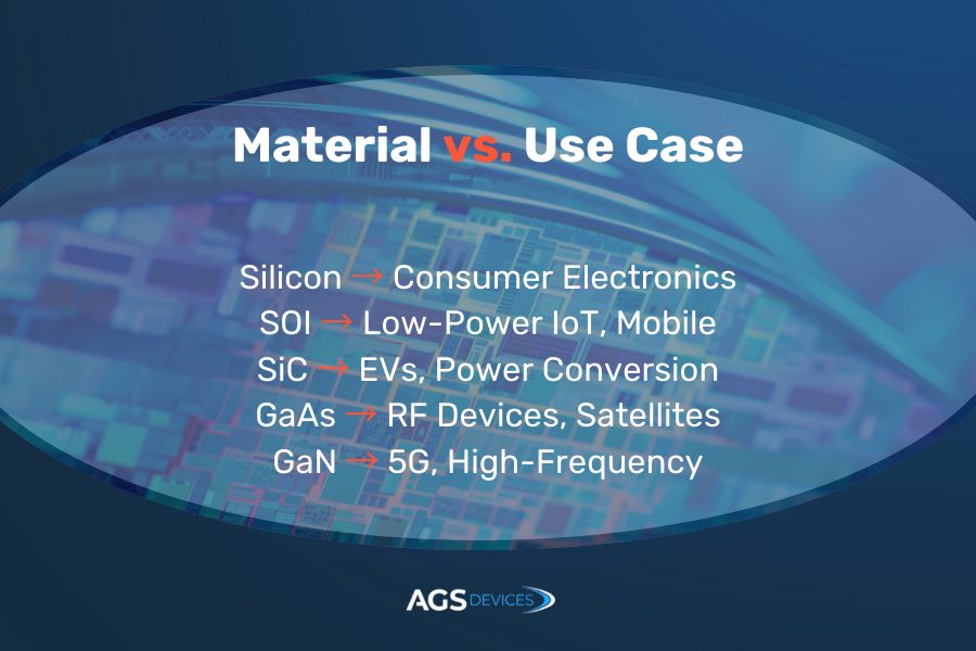
Use case: Most computer processors and mobile chips are built on CZ wafers, while solar cells or power MOSFETs often rely on FZ due to purity demands.
SOI Wafers (Silicon-on-Insulator)
Silicon-on-insulator (SOI) wafers feature a thin layer of silicon on top of an insulating layer (usually silicon dioxide), bonded to a silicon base.
This layered structure reduces parasitic capacitance and improves overall performance.
Benefits of SOI:
- Lower power consumption
- Faster switching speeds
- Improved thermal isolation
- Reduced leakage currents
- Common applications:
- High-speed processors
- RF communication chips
Fun fact: Apple’s A-series chips used in iPhones and iPads were early adopters of SOI technology for efficient mobile performance.
Compound Wafers: GaAs, SiC, GaN
For applications where traditional silicon falls short, compound semiconductor wafers step in with superior performance characteristics.
Gallium Arsenide (GaAs):
- Exceptional for high-frequency and optoelectronic devices
- Used in RF amplifiers, LEDs, and satellite communications
Silicon Carbide (SiC):
- Withstands higher voltages and temperatures than standard silicon
- Ideal for EV powertrains, solar inverters, and industrial motor drives
Gallium Nitride (GaN):
- Supports high efficiency and fast switching speeds
- Common in radar systems, 5G base stations, and fast-charging devices
Key Characteristics That Define Wafer Quality
Not all semiconductor wafers are created equal. The performance, yield, and reliability of a chip often come down to the wafer it’s built on.
Key factors engineers and procurement specialists look for are:
- Surface flatness and roughness: Wafers must be incredibly flat to ensure proper photolithography alignment and uniform material deposition. Even nanometer-scale variations can affect device performance. Ultra-flat wafers minimize defects and support higher transistor densities — especially important in advanced nodes below 10nm.
- Crystallographic orientation: Orientation refers to how atoms are arranged within the wafer’s crystal structure (e.g., (100), (111)). This orientation affects etching behavior, dopant diffusion, and mechanical properties. For example, (100) orientation is preferred in CMOS fabrication due to its ease of processing and smoother oxide interfaces.
- Resistivity and doping concentration: The wafer’s electrical resistance — determined by its doping level and material purity — affects current flow and device behavior. Low-resistivity wafers are typically used in high-speed logic circuits, while high-resistivity wafers are better suited for RF and sensor applications.
- Defect density: Crystal defects like dislocations, stacking faults, or micro-pits can significantly reduce wafer yield and device reliability. High-quality wafers have low defect densities, ensuring higher chip performance and fewer failures during manufacturing.
- Dielectric strength and insulation quality: Especially important in power devices, dielectric strength determines a wafer’s ability to withstand high voltages without breakdown. This is critical for applications in electric vehicles, solar inverters, and industrial automation.
- Thermal conductivity: A wafer’s ability to dissipate heat directly impacts device longevity and reliability. Materials like SiC and GaN outperform silicon in this area, making them ideal for power electronics where thermal stress is a major concern.
Semiconductor Wafer Guide: Key Takeaways
- Choosing the right wafer thickness can improve chip efficiency, reduce warping during fabrication, and meet thermal/mechanical demands.
- Beyond silicon, SOI and compound materials enable cutting-edge applications like AI, high-speed communications, and power electronics.
- Key specifications like Total Thickness Variation (TTV), crystal structure, and resistivity should guide procurement decisions.
- Knowing where wafers are made — and by whom — can help companies avoid delays and maintain continuity in production.
Why AGS Devices Is a Trusted Partner for Semiconductor Components
At AGS Devices, we understand that every high-performing electronic system starts with a reliable foundation—quality components.
From sourcing advanced semiconductor wafers to supporting full-scale BOM management, our mission is to deliver components that meet today’s performance demands and tomorrow’s innovation.
We also support your full component sourcing needs, offering:
- BOM Management
- Shortage and Obsolescence Solutions
- Sourcing and Procurement
- Excess Material Acquisition
When performance, speed, and reliability matter, you need a sourcing partner that delivers more than parts — you need expertise, transparency, and a team that’s invested in your success.