P-type semiconductors are vital components in industries ranging from renewable energy to consumer electronics.
They also play a major role in power regulation, signal processing, and energy-efficient devices, as they make modern technology faster and smarter.
Have you ever asked yourself how solar panels work? The simple answer is the power of P-type semiconductors, which create the foundation for photovoltaic cells that can turn sunlight into power.
Today, we’ll explain what P-type semiconductors are, how they work, and cover their most common properties and applications.
What Is a P-Type Semiconductor?
Conductors that enable efficient charge flow in transistors, diodes, and integrated circuits are typically P-type semiconductors.
Unlike standard conductors, semiconductors rely on a process called doping, which modifies their electrical properties to improve performance.
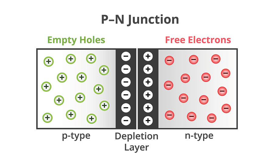
In a P-type semiconductor, doping introduces acceptor atoms — elements with one fewer valence electron than the base material (typically silicon or germanium).
These acceptors create “holes,” or positive charge carriers, that move through the material when an electric field is applied.
How P-Type Semiconductors Differ From N-Type
All semiconductors fall into one of two categories: P-type or N-type.
While P-type semiconductors depend on positive charge carriers (holes), N-type semiconductors use free-moving electrons to conduct electricity.
Think of it like this:
- P-type: The absence of electrons creates “holes,” which behave like positive charges moving through the material.
- N-type: Excess electrons move freely, enabling current flow.
How P-Type Semiconductors Are Made
The process of creating P-type semiconductors starts with pure silicon or germanium, both of which are naturally intrinsic semiconductors — meaning they don’t conduct electricity well on their own.
The Doping Process: Introducing Acceptors
To make a P-type semiconductor, the base material is doped with acceptor atoms, typically from group III elements in the periodic table, such as boron (B), aluminum (Al), or gallium (Ga).
These elements have three valence electrons, while silicon and germanium have four.
When an acceptor atom replaces a silicon atom in the crystal lattice, it creates a “hole” — a missing electron that acts as a positive charge carrier. These holes then attract electrons that are nearby, allowing current to flow through the material when voltage is applied.
Common P-Type Materials
- Silicon (Si): The most used semiconductor material because of its abundance, stability, and compatibility with modern fabrication processes.
- Germanium (Ge): This material is less common but still used in some applications due to its high electron mobility — though it’s more sensitive to temperature fluctuations than silicon.
- Gallium arsenide (GaAs): A compound semiconductor used in high-speed electronics and optoelectronics, offering superior performance over pure silicon
Key Properties and Electrical Behavior of P-Type Semiconductors
As we mentioned above, P-type semiconductors are largely used in modern electronics, enabling controlled electrical conduction in devices like different types of diodes, transistors, and integrated circuits.
Here, we’re going to talk in-depth about their properties and electrical behavior.
Hole Conduction vs. Electron Flow
In P-type semiconductors, the primary charge carriers are holes, while in N-type semiconductors, electrons carry the charge.
Here’s how the conduction process differs:
- P-type (hole conduction): When voltage is applied, electrons jump from atom to atom to fill these holes, making the holes appear to move through the material. This movement of holes in one direction mimics the flow of positive charge.
- N-type (electron flow): On the other hand, N-type semiconductors have excess electrons that move freely, carrying a negative charge through the material.
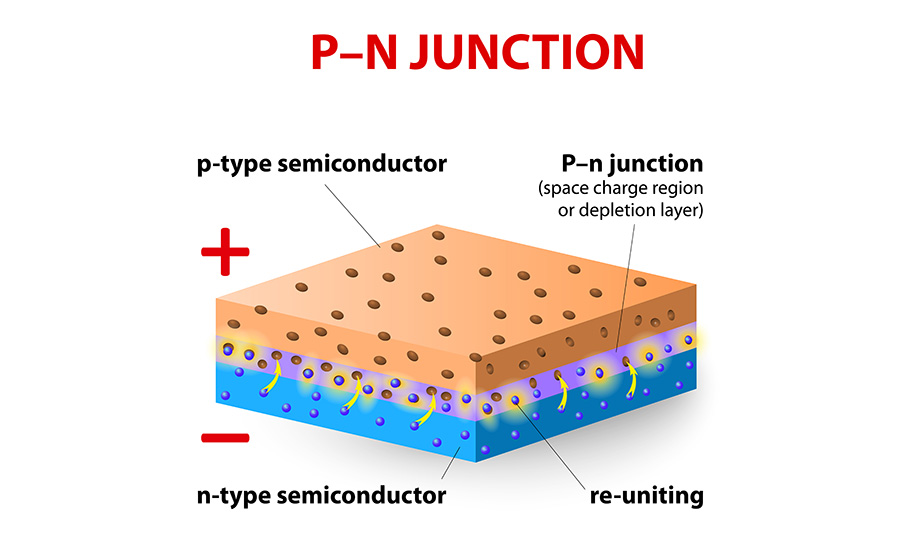
This fundamental difference is why P-type and N-type materials are combined in semiconductor devices like PN junctions, which enable critical functionalities such as rectification, amplification, and switching.
Impact on Electrical Performance and Efficiency
The electrical behavior of P-type semiconductors influences various industries that are dependent on electrical performance such as high-speed computing.
Key factors include:
- Conductivity: P-type materials usually have lower electron mobility than N-type semiconductors, which makes them less conductive under the same conditions. However, their behavior in junctions makes them essential for balancing circuit performance.
- Efficiency: P-type semiconductors are optimized for energy-efficient operation in devices like solar cells and low-power electronics, where hole conduction plays a crucial role.
- Thermal stability: P-type materials generally perform well in high-temperature environments, which makes them ideal for applications in automotive electronics and industrial systems.
Applications of P-Type Semiconductors in Modern Electronics
The ability of these semiconductors to conduct electricity through hole movement makes them essential in many applications in the whole world.
Here, we’re going to list a few of the most important ones.
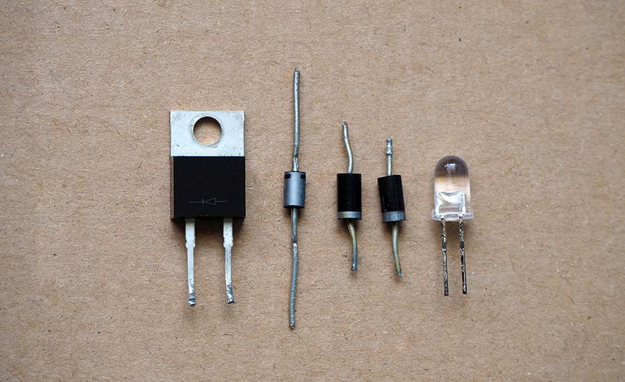
P-Type Semiconductors in Diodes and Transistors
Diodes and transistors rely on the interaction between P-type and N-type semiconductors to control electrical current.
This creates semiconductor devices like:
- PN junction diodes: The junction between P-type and N-type materials enables one-way current flow, making these diodes essential in power supplies, rectifiers, and signal modulation circuits.
- Bipolar junction transistors (BJTs): P-type materials are used in PNP and NPN transistors, where they enable switching, amplification, and digital logic operations. These transistors power everything from audio systems to industrial automation equipment.
- MOSFETs and power transistors: In power electronics, P-type transistors control high-voltage switching and energy-efficient power conversion in applications like electric vehicles and smart grids.
Integration in Microprocessors and ICs
P-type semiconductors are a core component of integrated circuits (ICs) and microprocessors, enabling complex digital operations in computers, mobile devices, and embedded systems.
They power essential digital technologies, including:
- Complementary metal-oxide-semiconductor (CMOS) technology: Modern microprocessors and memory chips rely on CMOS technology, which pairs P-type and N-type transistors to minimize power consumption and maximize processing speed.
- Logic gates and digital circuits: P-type transistors play a key role in logic circuits, helping to execute billions of computations in modern processors, AI chips, and data storage devices.
- Embedded systems: Many low-power embedded devices, such as smart sensors, IoT devices, and industrial controllers, use P-type semiconductors in low-energy, high-efficiency applications.
How P-Type Complements N-Type in Semiconductor Devices
P-type and N-type semiconductors are almost never used as separate components.
Instead, they work together in essential semiconductor components such as:
- PN junction diodes: The junction between P-type and N-type materials allows current to flow in one direction, making diodes essential for rectification and power conversion.
- Bipolar junction transistors (BJTs): These transistors consist of alternating P and N layers (NPN or PNP configurations), enabling signal amplification and switching.
- MOSFETs & power electronics: Many field-effect transistors (FETs) use a combination of P-type and N-type materials to control power flow efficiently in high-performance circuits.
- Solar cells & photovoltaics: P-type and N-type layers work together to convert sunlight into electrical energy, optimizing power generation in renewable energy applications.
Why Source P-Type Semiconductors From AGS Devices?
At AGS Devices, we know how important P-type semiconductors are for powering advanced electronics and that’s why our experts are here to help.
Our team at AGS follows rigorous quality control standards and works with trusted manufacturers to provide certified, high-performance semiconductors that meet industry demands.
Beyond semiconductors, we also supply other electronic components such as:
- Power Supply Distributors
- Optoelectronics
- Circuit Protection
- Interconnects
- Passive Components Electronics
- Electronic Testing Equipment
- Electromechanical Devices
![Semiconductor Wafer Guide [Thickness & Types]](https://www.agsdevices.com/wp-content/uploads/2025/04/semiconductor-wafer-hero-image.jpg)